JunPus thermal compounds deliver advanced heat dissipation solutions tailored for high-performance AI chips, CPUs, GPUs, and 5G base stations.
Engineered for cutting-edge semiconductor technologies,
our patented thermal pastes optimize thermal conductivity, ensuring stable performance under intensive workloads. Trusted across electronics, data centers, and telecommunications
Select the tape grade and process for your assembly. Application validation is required.
Adhesion · Fit · Electrical requirements
A dependable bond starts with the specification.
Secure attachment and electrical safety need their own design checks. Review the selected grade, thickness, surfaces and operating conditions before setting the limits.
Bond strength
Match adhesion to the actual surfaces and mechanical loads. Review peel resistance, holding or shear behaviour, bond area and ageing under the intended conditions.
Surface preparation + controlled application
Electrical insulation
Specify the isolation requirements for your assembly and request grade-specific electrical data. Avoid exposed contacts, sharp edges and damage to the tape.
Material data + assembly verification
Voltage qualification
A dielectric breakdown result is not a working-voltage rating. Confirm the test method, material thickness and applicable design requirements before qualification.
Defined conditions + application validation
No universal electrical-insulation or voltage rating is stated for the current product family. Ask JunPus for the current documentation of the selected grade.
Two adhesive faces. One planned interface.
The tape remains between the two mating surfaces. The release liner protects the adhesive during handling and is removed before that side is bonded. It is not a cooling layer.
Release-liner configuration depends on the supplied grade.
Thermal tape: stays in the interfaceRelease liner: removedHardware: mating surfaces
Start with the actual assembly.
Different products create different bonding problems. The following concepts show the exact contact location for each application family, with qualification needs kept visible.
Lighting & illumination
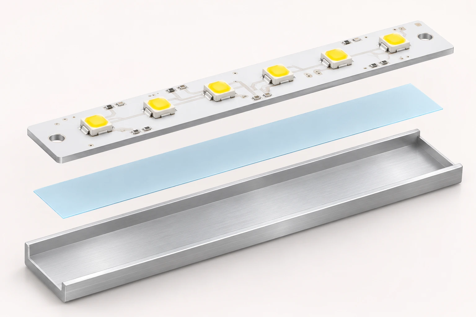
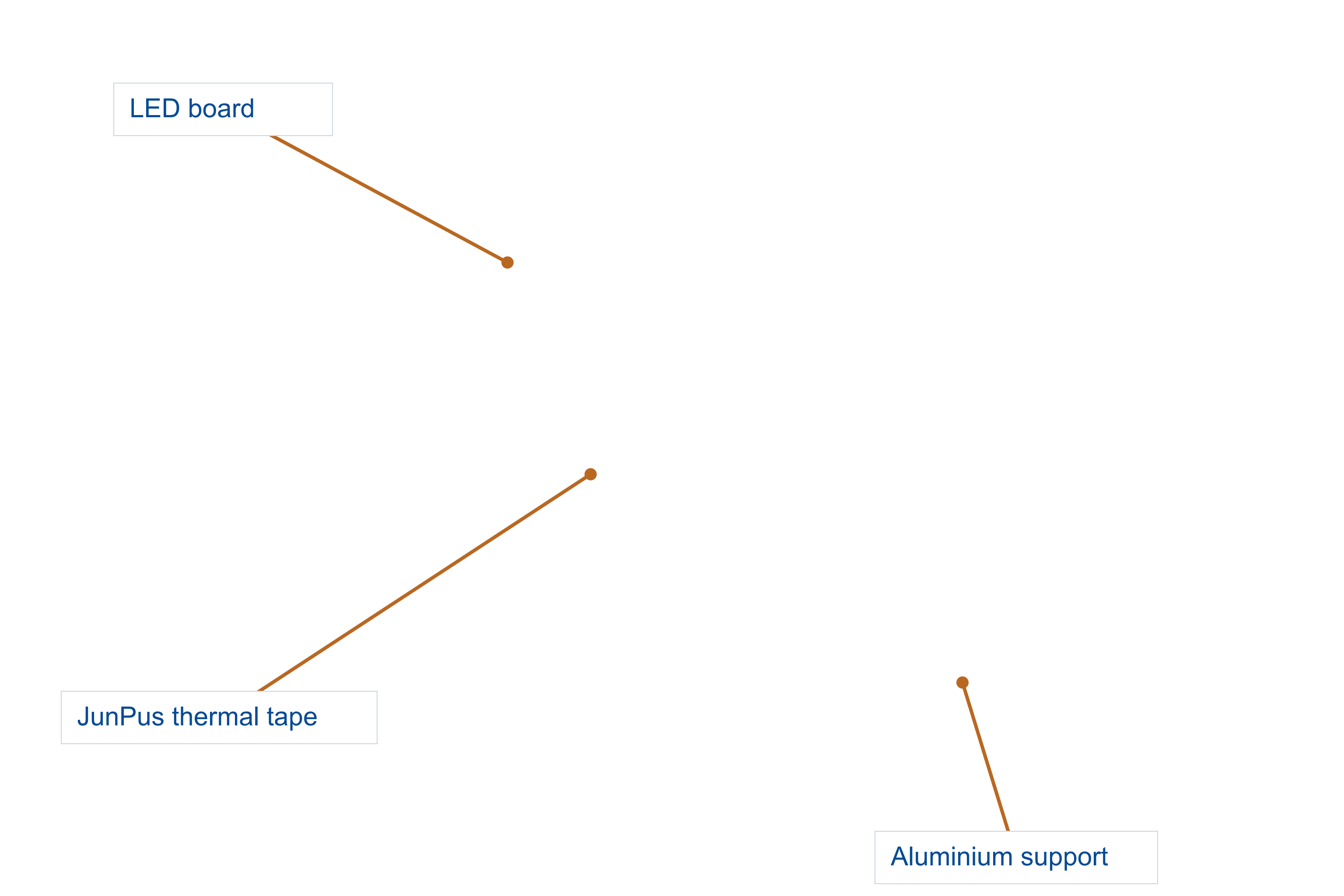
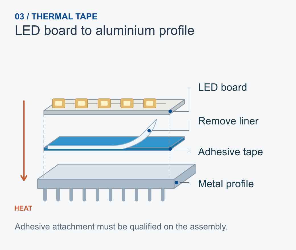
LED board. Aluminium support.
Bond the flat backside of an LED metal-core board to its designed aluminium heat-spreading surface. Keep the adhesive away from LEDs, optics and electrical contacts.
Thermal tape bonds the two flat contact surfaces shown below.
LED board backsideMetal-core board, components face outward
JunPus thermal tapeGrade selected for this interface
Where to evaluate itLight bars, linear lighting and selected luminaire board-to-housing interfaces. Match the tape footprint to the thermal contact area, not the illuminated face.
What must be checkedBoard flatness, surface finish, electrical clearances, bond area, thermal cycling and the luminaire’s retention requirements.
Compact electronics & network hardware
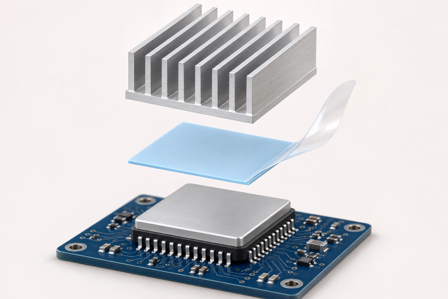
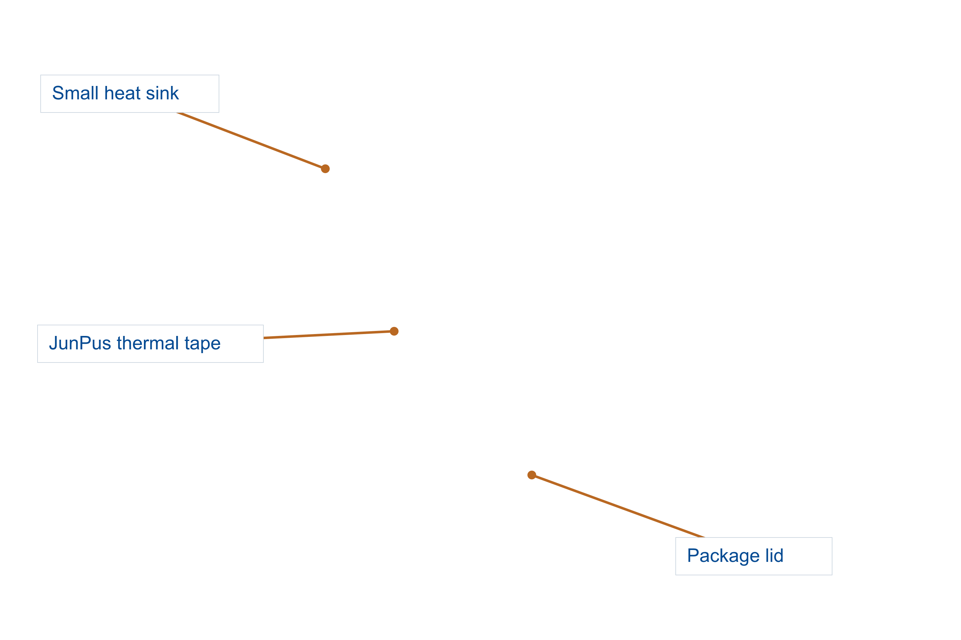
Small heat sink. Defined contact area.
Evaluate a lightweight heat sink attached to a suitable flat package lid or a designed heat-spreading surface. The tape sits beneath the sink base, not across nearby components.
Thermal tape bonds the two flat contact surfaces shown below.
Small heat sinkFlat underside of the heat-sink base
JunPus thermal tapeBonding and thermal interface
Package lid / spreaderSuitable flat thermal contact face
Where to evaluate itCompact controllers, networking hardware and edge electronics where a small heat sink needs a defined bonded interface. Not a blanket recommendation for every processor.
What must be checkedPackage surface and allowable load, heat-sink mass, shear/peel forces, vibration, rework needs and actual junction temperature under load.
Power electronics & electrification
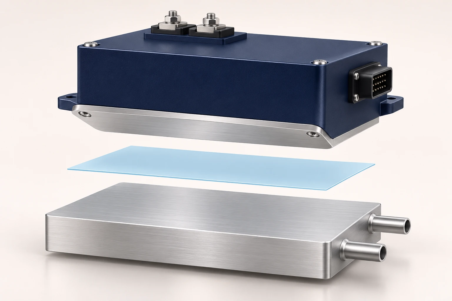
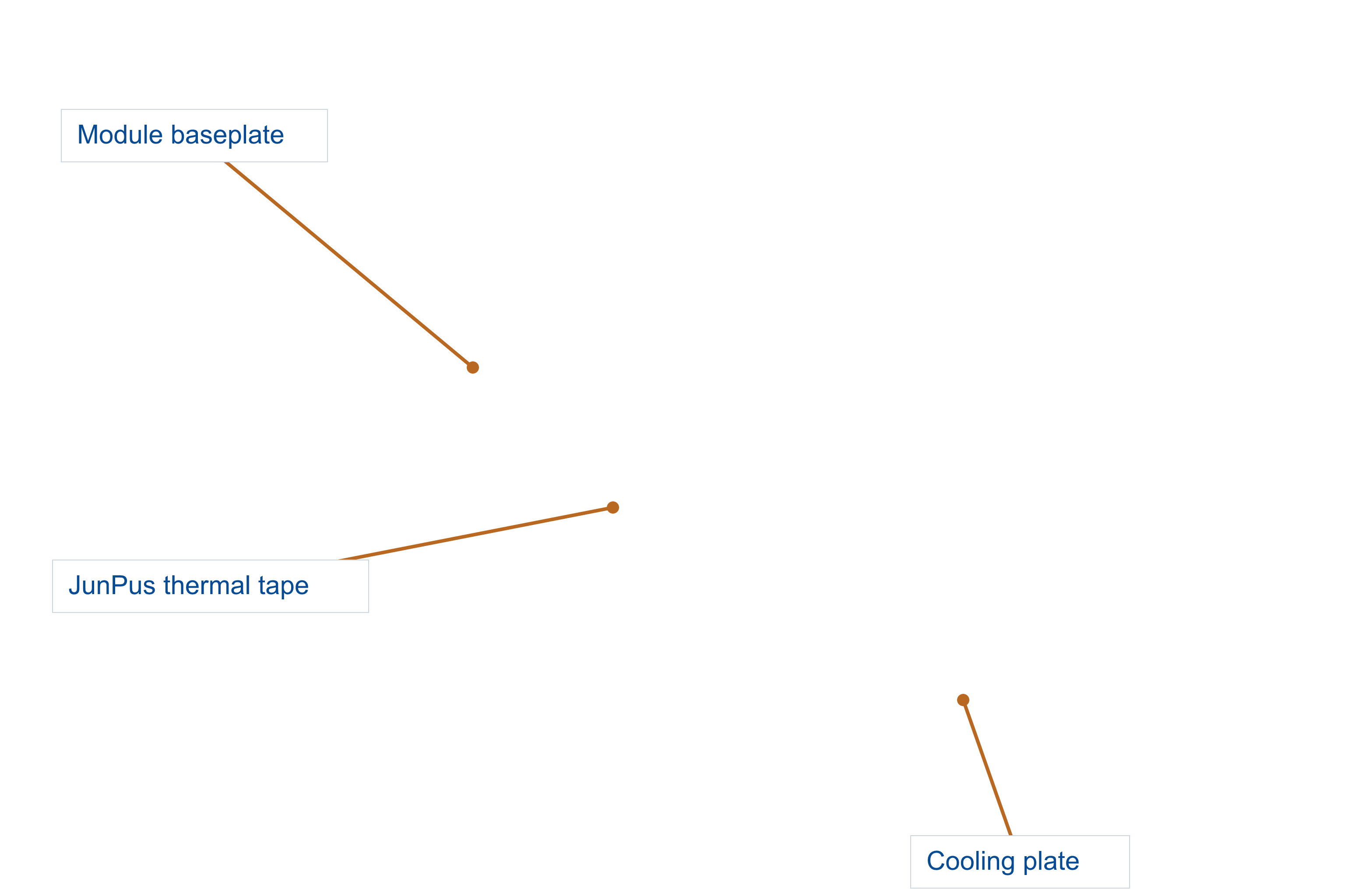
Module baseplate. Cooling surface.
A conditional engineering concept for bonding a flat module baseplate to a cooling plate. Treat thermal, electrical and mechanical qualification as a combined design task.
Thermal tape bonds the two flat contact surfaces shown below.
JunPus thermal tapeOnly after grade and process validation
Cooling plateDesigned heat-rejection surface
Where to evaluate itPower-electronics assemblies used in industrial drives, charging and energy systems.
What must be checkedElectrical isolation, sustained temperature, coolant-system design, bond durability, service loads, retention and safety requirements. Do not replace specified fasteners or battery protection layers.
Battery module thermal management
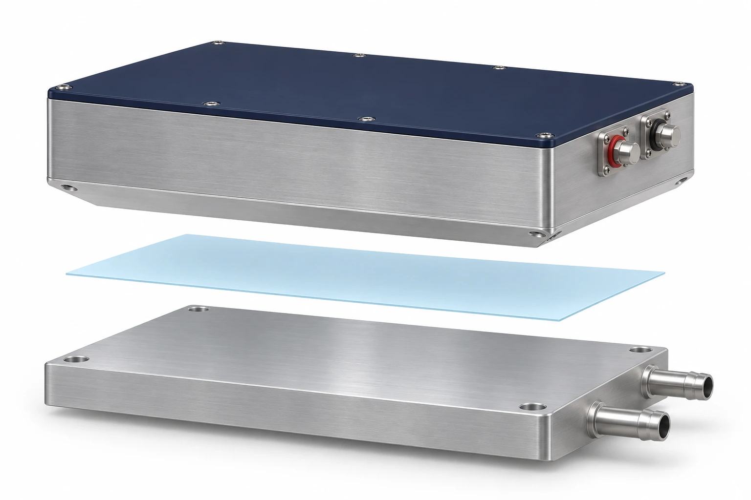
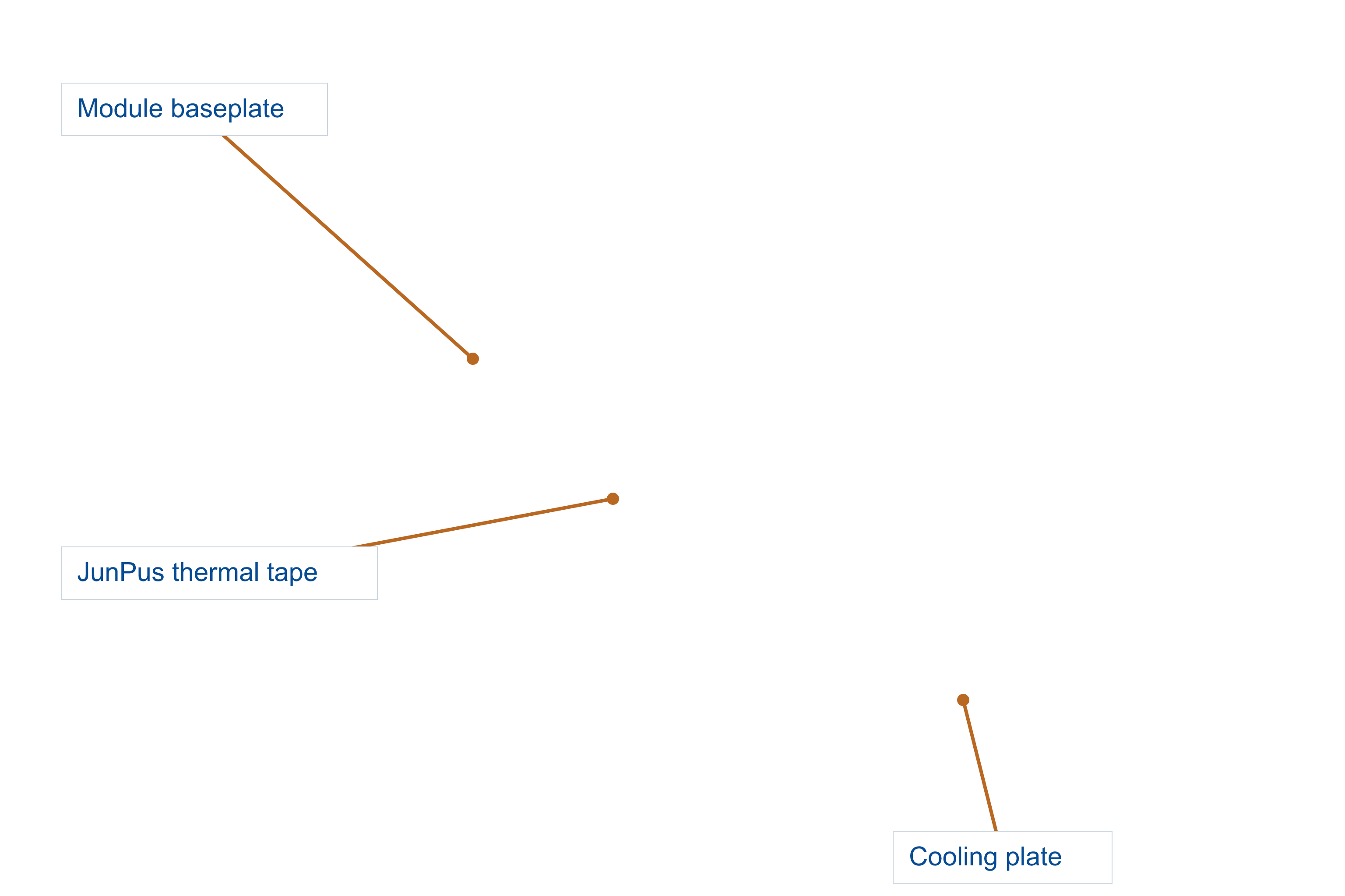
Module baseplate. Cooling plate.
Evaluate the external, designed thermal contact face of a battery module against its cooling plate. This is a system-level engineering question, not a universal direct-cell adhesive recommendation.
Tape location: between the designed module base and cooling plate.
Module contact faceDesigned external baseplate
JunPus thermal tapeConditional: grade and system validation
Cooling plateDesigned thermal contact surface
Where to evaluate itModule-to-cooling-plate mounting for engineering discussion in electrification and energy-storage projects.
What must be checkedElectrical isolation, cell/module movement, thermal cycling, moisture, ageing, shear and peel loads, mechanical retention and battery-system safety. Tape is not a substitute for required fire barriers or cell insulation.
The selected grade must be evaluated in the actual assembly.
Precision converting & placement
The right length. The right width. A defined contact area.
Specify the footprint before removing the liner. The dimensions belong to your assembly drawing, including any cut-outs and electrical or mechanical clearances.
Length (L) and Width (W) are project inputs.
Define the geometry.
Confirm length, width, thickness, corner shape and cut-outs. Keep the specified bond area within the intended contact surfaces.
Protect the adhesive.
Keep the supplied protective liners in place during cutting where practical. Use a clean, controlled method without stretching or creasing the tape.
Inspect the edges.
Check the cut against the approved drawing. Avoid frayed edges, contamination, burrs, trapped liner and encroachment on contacts or fasteners.
Prepare. Peel. Place with purpose.
A clear reference sequence for a two-liner double-sided format. Follow the actual product label, technical data sheet and equipment instructions when the supplied format differs.
Before you begin
Power down and disconnect the equipment. Use the required ESD controls. Confirm the correct tape grade, surface compatibility and assembly method. Do not assume tape is electrically insulating or mechanically sufficient without the relevant data.
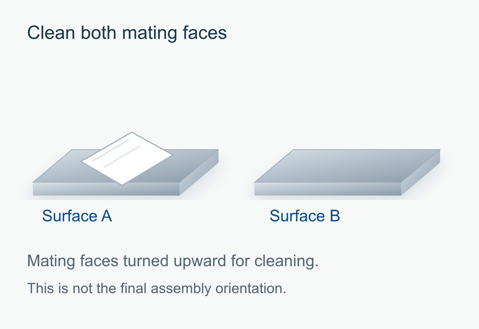
Clean both mating surfaces, not only one.
Clean and dry both faces.
Remove contamination and old material using the surface and equipment maker’s approved method. Let both faces dry completely. Do not touch the cleaned bond areas.
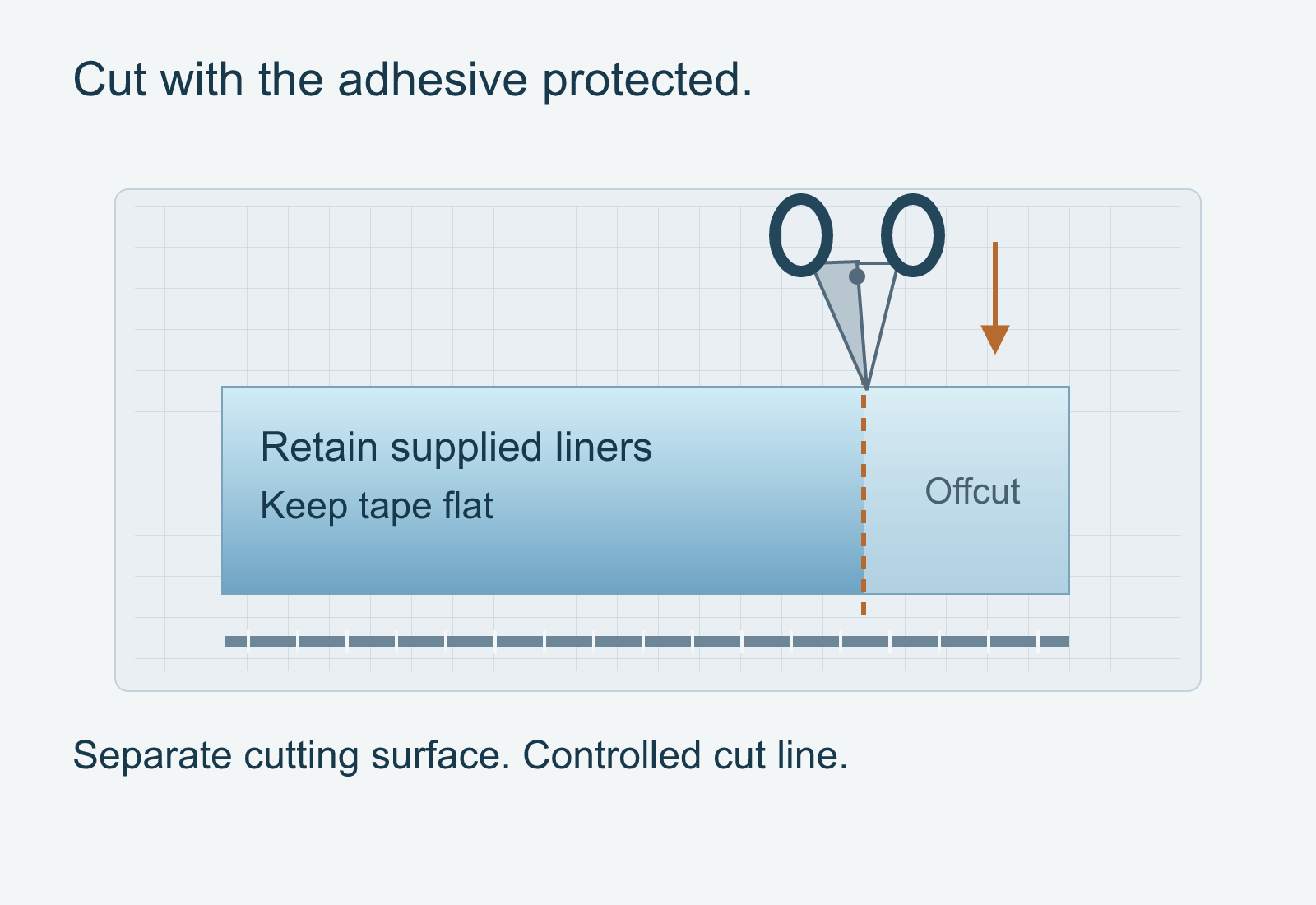
Confirm tools, dimensions and process for the selected grade.
Measure the footprint. Make the cut.
Confirm Length (L), Width (W) and the required profile against the assembly drawing. Cut on a suitable separate work surface with the liners retained where practical. Keep the tape flat and unstretched; protect cut-outs and clearances for leads, connectors and fasteners.
Two-liner example; follow the supplied roll or sheet format.
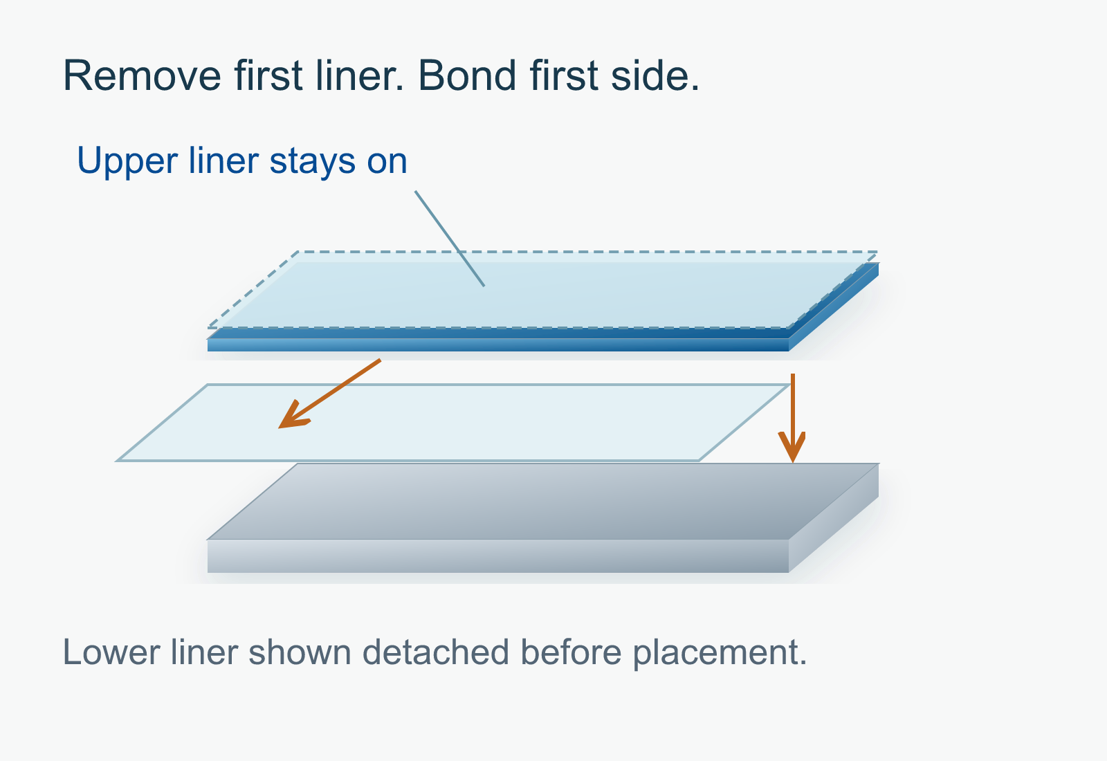
Bond the first side.
Remove the first release liner. Align the exposed adhesive to one prepared surface and apply it progressively, avoiding folds and trapped air. Keep the outer liner in place for handling.
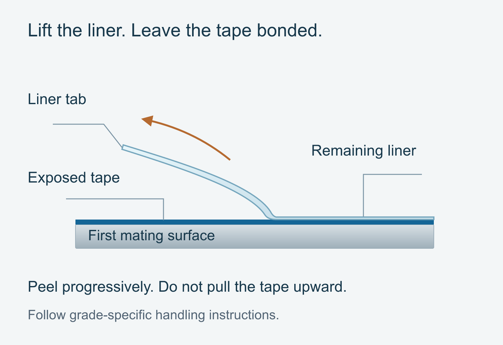
Liner lifts away; the functional adhesive layer stays bonded.
Peel the remaining liner.
Pinch only the liner tab. Peel it back progressively, following the grade-specific handling direction, while keeping the adhesive layer flat on the first surface. Do not pull the tape upward or touch the exposed bond area.
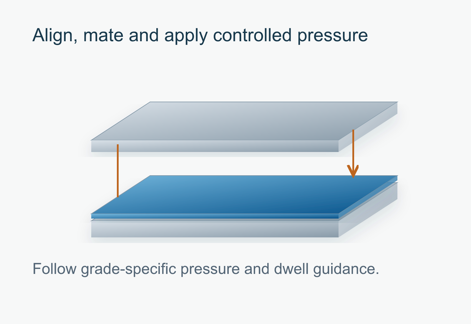
No universal pressure or dwell time is claimed.
Align and make contact.
Bring the second surface into alignment before contact. Seat it evenly and apply the pressure, time and temperature specified for the selected grade and assembly.
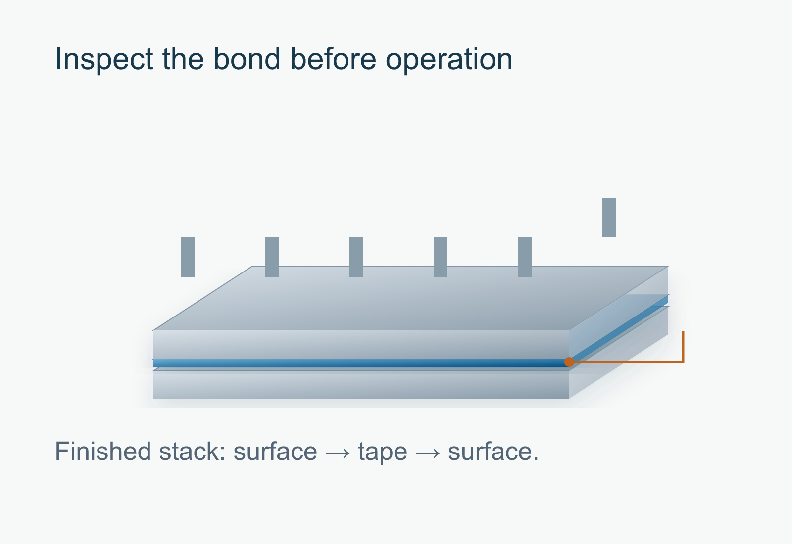
Final sandwich: mating surface → tape → mating surface. No liner.
Inspect, then qualify.
Check alignment, full intended contact and any specified retention. Validate adhesion, thermal performance and durability in representative operating conditions before release.
Four checks. Before the build.
This checklist supports preparation. It does not approve a material or replace engineering validation.
0 of 4 checks reviewed
Define the grade. Confirm the details.
Share your actual interface with JunPus. A thermal-conductivity value alone does not establish suitability for a bonded assembly.
Current website family
High-Performance Thermal Tape
Product type
Thermally conductive adhesive tape
Grade / model
Confirm with JunPus for the intended application
Dimensions & format
Confirm thickness, width, length and converting options
Thermal & adhesion data
Request grade-specific values and test conditions
Electrical requirements
Request grade- and thickness-specific insulation / voltage data with test conditions
Process & compliance
Request handling guidance and applicable documents
Bring the assembly details.
Tell us the two surface materials, contact footprint, gap or flatness limits, thermal load, operating environment, retention needs and planned quantities. Include any required electrical isolation, rework or qualification criteria.
No release liner should remain between the bonded surfaces. A liner protects the adhesive before use. Its colour is not enough to identify the functional tape layer; follow the supplied product instructions.
Can I stack tape to fill a larger gap?
Do not stack layers by default. Additional interfaces change heat transfer and bonding behaviour. Ask JunPus to review the actual gap and select a suitable material and thickness.
Can thermal tape replace screws or clips?
Only when the assembly has been designed and validated for that attachment method. Do not remove specified mechanical retention, particularly for heavy heat sinks, vibration or safety-related assemblies.
Is every thermal tape electrically insulating?
No such assumption is made here. Obtain grade-specific dielectric and construction data, then evaluate the actual assembly’s voltage and safety requirements.
What if I need to reposition or remove it?
Repositioning can contaminate or damage the bond. Follow grade-specific rework and removal guidance. Do not pry fragile packages or reuse a removed piece without explicit approval from the material instructions.
Show us the two surfaces.
Start with your assembly, contact area and operating requirements. JunPus can discuss material options and the information needed for your evaluation.
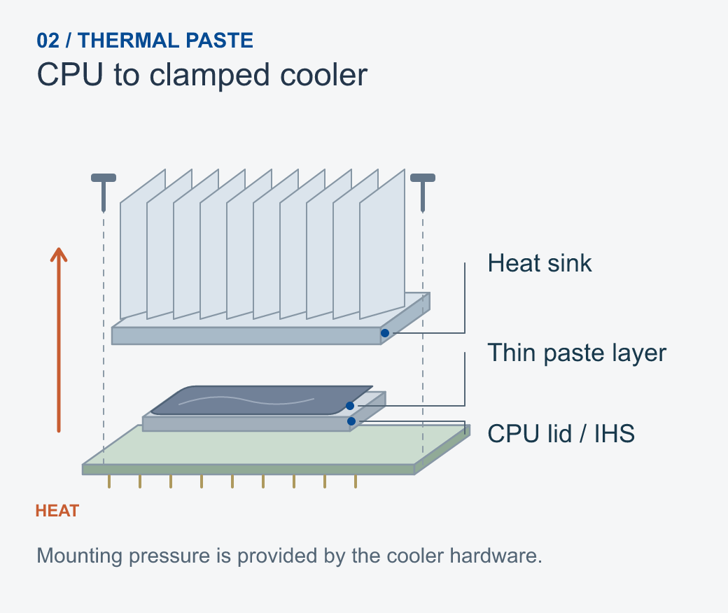
A graphics card, CPU cooler, LED light bar and compact circuit board need different interfaces. First check the gap, attachment method and assembly process.
Heat source→Selected interface material→Heat sink or spreader→System cooling
Thermal Pad
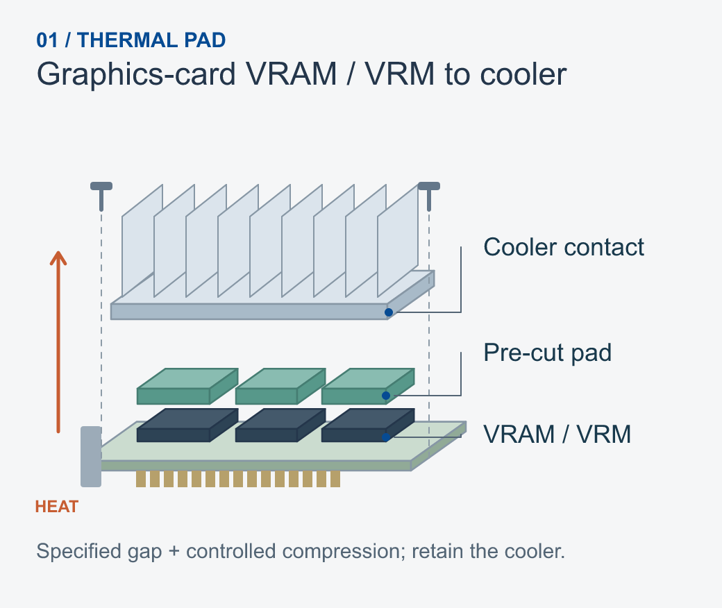
Fill a specified gap with a pre-cut piece.
Typical product
Graphics-card VRAM / VRM, SSDs and other assemblies with a designed component-to-cooler gap.
Material position
Component top → pad → cooler contact surface. The pad conforms under the specified compression.
Selection checks
First selection check
Match thickness, hardness and compression to the actual gap. Too much force can stress parts; insufficient contact leaves an ineffective heat path.
Keep in mind
Retain the designed mounting hardware. Surface tack does not make a pad an adhesive fastening tape.
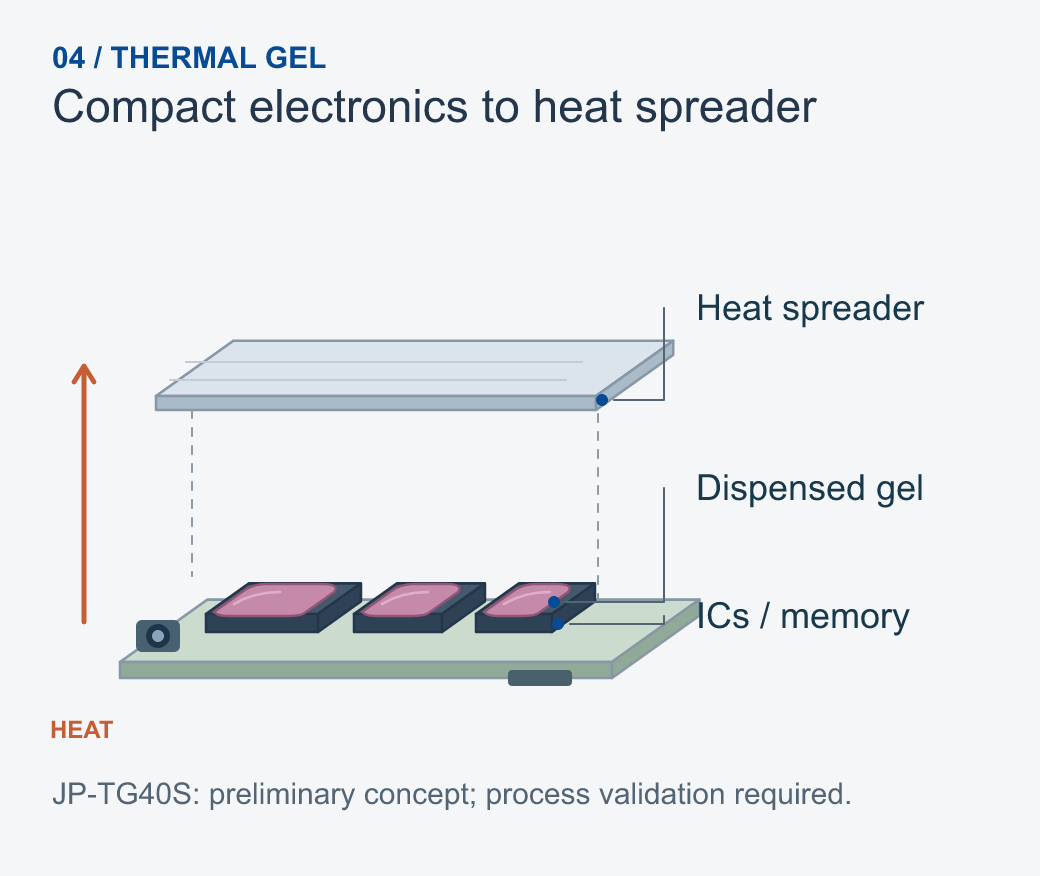
Patterned thermal contact with low assembly stress.
Typical product
Smartphone AP, PMIC and memory interfaces, compact PCB assemblies and sensor modules with pressure-sensitive components.
Material position
On defined chip or component contact areas, connecting them to a metal frame, heat spreader or housing.
Selection checks
Why this interface needs it
Dispensing or screen printing can place material only where it is needed. The soft-gel concept targets controlled contact with low mechanical stress.
Selection boundary
For JP-TG40S, confirm final layer thickness, dispense pattern, curing, reliability and released documentation. It is not presented as an adhesive fastener.
Choose the interface, not just the product label. One device may use different thermal materials in different locations. Do not substitute Tape, Gel or Pad for a CPU/GPU’s specified primary interface without engineering validation.
Gel is preliminary: review its selection limits
About the Gel illustration. JP-TG40S content follows the Preliminary Industrial TDS, Draft B, April 2026. It describes a proposed application window, not final released performance or certifications. Gels differ by formulation: another supplier’s large-gap or no-cure claims do not establish JP-TG40S capability.
Explore related JunPus products.
Use the material guide above to compare the contact design, then open the relevant product information.